Organic photorefractive materials
From Wikipedia, the free encyclopedia
Organic photorefractive materials are materials that exhibit a temporary change in refractive index when exposed to light. The changing refractive index causes light to change speed throughout the material and produce light and dark regions in the crystal. The buildup can be controlled to produce holographic images for use in biomedical scans and optical computing. The ease with which the chemical composition can be changed in organic materials makes the photorefractive effect more controllable.
Although the physics behind the photorefractive effect were known for quite a while, the effect was first observed in 1967 in LiNbO3.[1] For more than thirty years, the effect was observed and studied exclusively in inorganic materials, until 1990, when a nonlinear organic crystal 2-(cyclooctylamino)-5-nitropyridine (COANP) doped with 7,7,8,8-tetracyanoquinodimethane (TCNQ) exhibited the photorefractive effect.[2][3][4] Even though inorganic material-based electronics dominate the current market, organic PR materials have been improved greatly since then and are currently considered to be an equal alternative to inorganic crystals.[5]
Theory
There are two phenomena that, when combined together, produce the photorefractive effect. These are photoconductivity, first observed in selenium by Willoughby Smith in 1873,[6] and the Pockels Effect, named after Friedrich Carl Alwin Pockels who studied it in 1893.[7]
Photoconductivity is the property of a material that describes the capability of incident light of adequate wavelength to produce electric charge carriers. The Fermi level of an intrinsic semiconductor is exactly in the middle of the band gap. The densities of free electrons n in the conduction band and free holes h in the valence band can be found through equations:[8]

and

where Nc and Nv are the densities of states at the bottom of the conduction band and the top of the valence band, respectively, Ec and Ev are the corresponding energies, EF is the Fermi level, kB is the Boltzmann constant and T is the absolute temperature. Addition of impurities into the semiconductor, or doping, produces excess holes or electrons, which, with sufficient density, may pin the Fermi level to the impurities' position.[9]

A sufficiently energetic light can excite charge carriers so much that they will populate the initially empty localized levels. Then, the density of free carriers in the conduction and/or the valence band will increase. To account for these changes, steady-state Fermi levels are defined for electrons to be EFn and, for holes, EFp. The densities n and h are, then equal to


The localized states between EFn and EFp are known as 'photoactive centers'. The charge carriers remain in these states for a long time until they recombine with an oppositely charged carrier. The states outside the EFn − EFp energy, however, relax their charge carriers to the nearest extended states.[8]
The effect of incident light on the conductivity of the material depends on the energy of light and material. Differently-doped materials may have several different types of photoactive centers, each of which requires a different mathematical treatment. However, it is not very difficult to show the relationship between incident light and conductivity in a material with only one type of charge carrier and one type of a photoactive center. The dark conductivity of such a material is given by

where σd is the conductivity, e = elementary charge, Nd and N+
d are the densities of total photoactive centers and ionized empty electron acceptor states, respectively, β is the thermal photoelectron generation coefficient, μ is the mobility constant and τ is the photoelectron lifetime.[8] The equation for photoconductivity substitutes the parameters of the incident light for β and is

in which s is the effective cross-section for photoelectron generation, h is the Planck constant, ν is the frequency of incident light, and the term I = I0e−αz in which I0 is the incident irradiance, z is the coordinate along the crystal thickness and α is the light intensity loss coefficient.[8]
The electro-optic effect is a change of the optical properties of a given material in response to an electric field. There are many different occurrences, all of which are in the subgroup of the electro-optic effect, and Pockels effect is one of these occurrences. Essentially, the Pockels effect is the change of the material's refractive index induced by an applied electric field. The refractive index of a material is the factor by which the phase velocity is decreased relative to the velocity of light in vacuum. At a microscale, such a decrease occurs because of a disturbance in the charges of each atom after being subjected to the electromagnetic field of the incident light. As the electrons move around energy levels, some energy is released as an electromagnetic wave at the same frequency but with a phase delay. The apparent light in a medium is a superposition of all of the waves released in such way, and so the resulting light wave has shorter wavelength but the same frequency and the light wave's phase speed is slowed down.[10]
Whether the material will exhibit Pockels effect depends on its symmetry. Both centrosymmetric and non-centrosymmetric media will exhibit an effect similar to Pockels, the Kerr effect. The refractive index change will be proportional to the square of the electric field strength and will therefore be much weaker than the Pockels effect. It is only the non-centrosymmetric materials that can exhibit the Pockels effect: for instance, lithium tantalite (trigonal crystal) or gallium arsenide (zinc-blende crystal); as well as poled polymers with specifically designed organic molecules.[11]
It is possible to describe the Pockels effect mathematically by first introducing the index ellipsoid – a concept relating the orientation and relative magnitude of the material's refractive indices. The ellipsoid is defined by
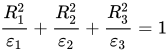
in which εi is the relative permittivity along the x, y, or z axis, and R is the reduced displacement vector defined as Di/√8πW in which Di is the electric displacement vector and W is the field energy. The electric field will induce a deformation in Ri as according to:
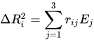
in which E is the applied electric field, and rij is a coefficient that depends on the crystal symmetry and the orientation of the coordinate system with respect to the crystal axes. Some of these coefficients will usually be equal to zero.[10]


